As described in the previous part, in computers a transistor acts as a switch and either lets electricity through or it doesn’t. Being able to conditionally let electricity through, means you can work with two discrete values: electricity and no electricity. This literally translates directly to a bit: 1 means electricity (typically +3.5V to +5V) and 0 means no electricity (0V). This simple fact gives us the ability to build logic.
In high level languages, you typically have some sort of boolean data type. This is called as such because it is used in boolean logic (and, or, xor, not, etc.) and is a result of boolean algebra named after George Boole.
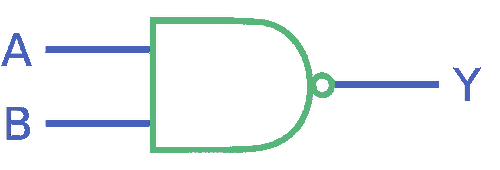
At a hardware level, this boolean logic is implemented through logic gates. Using two of the transistors we discussed earlier, we can construct our first logic gate: the NAND (negative and) gate. It behaves like this: if and only if both of the transistors in the gate are conducting (i.e. both inputs are 1), will the NAND gate result be 0. Otherwise, it will be 1.
The logic table for NAND is as follows, where A and B are the two transistors and Y is the output of the gate:
NAND
----------
A  B  |  Y
----------
0  0  |  1
0  1  |  1
1  0  |  1
1  1  |  0
And this is the symbol:
The reason the NAND gate is so important is because all other gates can be built by using one or more of them (the same goes for NOR gates, by the way).
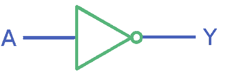
NOT gate
A NOT gate can be built by using a NAND gate where both inputs are the same value (i.e. wired together) so A = B. Using the above table, this means a 0 (two zeroes wired together) will become a 1 and a 1 (two ones wired together) will become a 0. Which is the NOT logic we wanted.
NOT
-------
A  |  Y
-------
0  |  1
1  |  0
And this is the symbol:
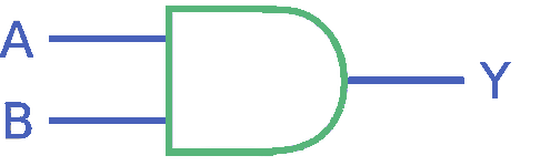
AND gate
An AND gate can be built using a NAND gate and a NOT gate (which is basically a double negative): if both inputs are 1, an AND gate should yield a 1, which is the negated result of a NAND gate, which returns a 0 in that case. Using the NOT gate after the NAND gate inverts that value, yielding a 1.
AND
----------
A  B  |  Y
----------
0  0  |  0
0  1  |  0
1  0  |  0
1  1  |  1
And this is the symbol:
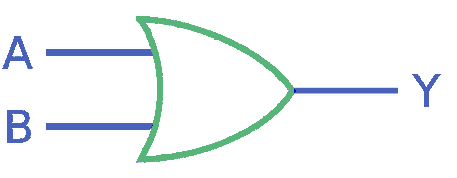
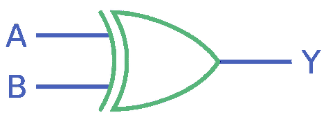
OR gate
An OR gate can be built using two NOT gates that negate the two inputs to a NAND gate: if both inputs are 0, negating them to 1 and inputting them to a NAND gate will return a 0. In other cases, it will return a 1, as matches the OR table below.
OR
----------
A  B  |  Y
----------
0  0  |  0
0  1  |  1
1  0  |  1
1  1  |  1
And this is the symbol:
XOR gate
A XOR gate only returns 1 if either input is 1. If both are 0 or 1, it will return 0. It can be built using 3 NAND gates chained up, with two NOT gates before that.
XOR
----------
A  B  |  Y
----------
0  0  |  0
0  1  |  1
1  0  |  1
1  1  |  0
And this is the symbol:
Remembering a single bit
The most essential thing we can build with NAND gates is computer memory. Using only 4 gates and specific wiring, it is possible to “remember” a single bit. The trick is that an additional setter input s is used on the first gate 1 in the sequence, and only if s is 1, will input i have any effect on output o of the memory cell:
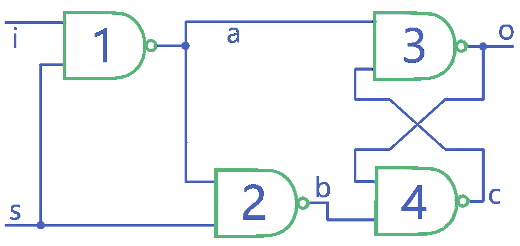
Let’s put that to the test:
With i = 0 and s = 1, it follows that:
- Gate 1 receives i = 0 and s = 1 and outputs a = 1
- Gate 2 receives a = 1 and s = 1 and outputs b = 0
- Gate 4 receives b = 0 and will output c = 1
- Gate 3 receives a = 1 and c = 1 and will return the final output o = 0
- Thus: o = i
With i = 1 and s = 1 it follows that:
- Gate 1 receives i = 1 and s = 1 and outputs a = 0
- Since a = 0 for both gate 2 and gate 3, gate 2 outputs b = 1 and gate 3 outputs o = 1
- Gate 4 now receives b = 1 and o = 1 and outputs c = 0
- Gate 3 receives back c = 0 and will always output o = 1
- Thus: o = i
So when s = 1, output o always equals input i.
If s = 0, the second input to gate 1 will always be 0, thus always yielding a = 1. No matter how we change i, a will always be 1 because the second input s = 0. The same applies to gate 2: it doesn’t care about the value of a because s = 0 and b will therefore always be 1.
What we really care about here is what the value of output o is. This depends on the “remembered” value from before s became 0. If i and o were 0, gate 3 must have had both inputs set to 1 (or it wouldn’t yield o = 0) and gate 4 had both inputs set to 0 (b = 0 because a and s are 1, o = 0 because of gate 3). If we switch s off and it becomes 0, b becomes 1, but since o is still 0, the output of gate 4 will still be 1 and nothing changes.
The same logic applies when i and o were 1 before s became 0: a was 0 because i and s were 1, therefore b was 1 and therefore both inputs to gate 4 were 1, c was therefore 0 and both inputs to gate 3 (a and c) were 0, and output o = 1. If we switch s off and it becomes 0, a becomes 1 but since c is still 0, the output of gate 3 is still o = 1.
As you can hopefully tell from this, input i only has effect on output o when input s = 1. This is how 4 NAND gates can simulate “remembering” a single bit.
Register
A single bit only has two distinct values and is still not very practical. In 8-bit systems, eight of the memory cells we described above are combined into a byte and their setters are connected so a single byte can be written at the same time. Now, at some point, you want to do something with the output of this byte, or it wouldn’t make sense to remember anything.
To achieve that, eight AND gates are connected to each output of the byte and another input is introduced called the enabler. If the enabler is 0, AND will never return 1 and thus, no data is let through. If the enabler is 1, the byte will be passed through untouched (0 AND 1 = 0, 1 AND 1 = 1) and the data can be worked with.
This place to store and retrieve some memory is called a register and many of those exist inside a computer.
Bus
Every component inside a computer is connected through something called a bus. Each register is also connected to this bus and copying one register to another is done by first enabling the source register. What happens now is that the bus is actually the same value as the register. If we next set another register, this value is stored in the target register. Disabling the set bit on the target and the enable bit on the source “disconnects” these registers from the bus again.
This is how data is set in memory (including registers for operations to be carried out; more about that later).
Decoder
A decoder is something that is built out of NOT gates and AND gates which has 2^i outputs, where i is the number of inputs. Each input and the negated value of each input (through a NOT gate) are connected to AND gates in such a way that only one output of the decoder is 1 at a time and the rest is 0.
In random access memory (RAM), this is used for addressing. Let’s take a 16X16 grid of bytes (256 bytes in total). One 4X16 decoder is responsible for addressing the horizontal wires in the grid and one 4X16 decoder is responsible for addressing the vertical wires in the grid. At each intersection, a register exists as we described earlier where one byte of memory can be stored and read.
A separate register called the memory address register (MAR) will contain the memory address that we want to read or write: 4 output bits determine the horizontal wire and 4 output bits determine the vertical wire.
This is the principle of random access memory.
Now that we know how to store and read things, it is time to find out how to calculate something, which is also quite an essential part of a computer. Move on to the next part!