In this series, I will try to summarize the most fundamental parts of a computer and the physics behind them. While there is much more to say about them than I will here, I try to stay concise and to the point within the context of programming. This series is intended as a preliminary series to “Building a basic X86 kernel” that can be found here, although it can of course be seen as standalone information.
For the sake of simplicity, in later chapters everything will be about 8 bit systems. This basically means that 1 byte can be processed in a single clock cycle and registers and buses have 8 bits. Although modern architectures have more specialized and optimized ways of doing things, the basic principles still apply.
This series is a mix of my own knowledge complemented by a lot of online research. During the course of things, I also stumbled upon a book called “But, How Do It Know?" by J. Clark Scott, which is a recommended read if you want to know more details than I describe here.
So, let’s get started!
Electrons
Atoms are composed of a nucleus (neutrons and protons) and electrons orbiting that nucleus. Neutrons have no electric charge, protons have a positive electric charge and electrons have a negative electric charge. Opposite charges attract and equal charges repel. There are various different orbits around the nucleus in which electrons move and the most relevant of these orbits to this story is the valence shell. This is the outermost shell and defines a lot of the chemical properties of a material.
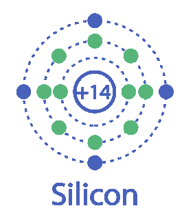
Silicon, for instance, has 4 valence electrons which have the tendency to bond with 4 nearby atoms (not necessarily other silicon atoms); this is called the covalent bond. The electrons will then be in the so called valence band and for conductivity to exist in semiconductors (to overcome the band gap), the electrons must be excited to jump from there to the conduction band.
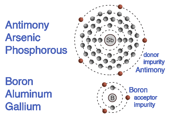
To excite electrons and make them jump and thus conduct electricity, we need free electrons and holes as charge carriers. To achieve that, a process called doping is applied to silicon where silicon atoms are replaced by atoms with more valence electrons (e.g. phosphorus which has 5) or less valence electrons (e.g. boron which has 3). This creates n-type (negative) and p-type (positive) silicon respectively: n-type has one free electron per phosphorus atom (donor impurity) because only 4 will bond with nearby atoms and p-type has one hole per boron atom (acceptor impurity) because we only have 3 electrons available. This creates the charge carriers we need. The more doping is applied, the more carriers will be available.
Diodes
A diode is an electronic component built from one p-type layer and one n-type layer joined together that lets electricity through in one direction but blocks it in the other. The edge of these layers is called the PN junction.
At the PN junction, the electrons in the n-type material jump over to the holes in the p-type material. This makes the edge of the p-type material slightly negatively charged and the edge of the n-type material slightly positively charged. The electric field that is now created blocks any natural progression of electrons through the material. It also creates a potential barrier of 0.7V that must be overcome before electrons can flow again.
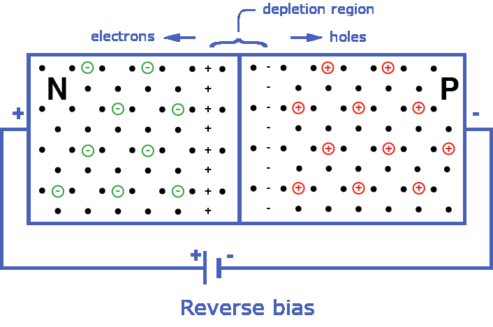
If you connect a negative charge to the p-type and the positive charge to the n-type, the holes in the p-type will be attracted to the negative charge and the electrons in the n-type will be attracted to the positive charge. This is called reverse bias and makes it impossible for electricity to flow through the diode any further: thus it blocks electricity in this direction.
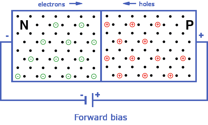
If we swap the charges and make the n-type negatively charged (with enough voltage to overcome the barrier), the electrons will cross the barrier and fill the holes in the p-type material and keep jumping holes towards the charge until it can join the external circuit: in this direction, electricity can flow just fine. This is called forward bias.
Transistors
Now, a transistor consists of three layers and is essentially two diodes joined together back to back, one NP diode and one PN diode, together forming an NPN transistor. The transistor has an NP and a PN junction that behave as a barrier as described earlier. One n-type layer is called the emitter, the other is called the collector. The p-type in between is called the base.
No matter how you connect a power source to the two n-types, one of the “diodes” will always be reverse biased and block electricity from flowing. This changes as soon as we connect a second power source (with enough power to overcome the potential barrier) to the base, like we did with the diode earlier. Now, electrons start flowing towards the positive charge of the base, but since many more electrons have made the jump to the p-type layer, those will be attracted by the positive charge of the other n-type, causing electricity to flow through the transistor.
Essentially within computers, the transistor acts as a switch. It can also be used to amplify current in different applications.
By the way, if you go to a DIY electronics store and ask for a transistor, you will be handed a small yet very visible funny looking tripod. In computer chips transistors are produced on a very (very) small scale instead (the current record is held by AMD’s Epyc Rome with almost 40 billion transistors on it).
Let’s move on to the next part to start using this conditional electricity!